Be ready on
For your needs

Advanced Materials for the Semiconductors, MEMS, Quantum, Displays.

wafer and Die handling up to 12 inch size

Vacuum wand, tweezers, Manual wand, pumps, ESD stand, Tubing and all related accessories.

ESD Safe PEEK, PPS, TEFLON, VESPEL materials, Lockable manual wand for 8 inch and 12 inch.

Negative Epoxy Dry
film Photo Resist

SUEX K Film thickness from 20um to 600um standard, Up to 1000um customizing. Precut size from 2 inch round, square to 12 inch and large panel size.

ADEX film from 5um to 75um, precut size and rolls.

etching Solutions

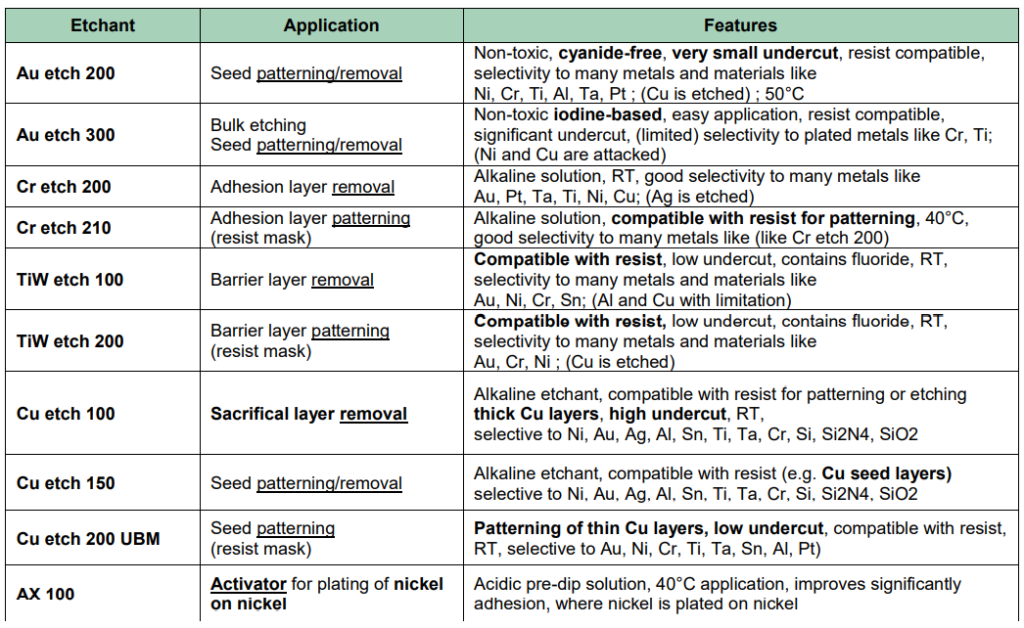
Etching Chemicals for the removal or pattering of metals.

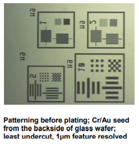
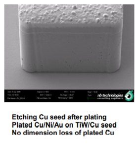
Sacrificial layers or Seed layers for electroplating, the seeds need to be removed after plating with selectivity to all other materials. The seeds need to be patterned before plating compatibility with masking resists.

image1

beta Ga2O3 single crystal

Single crystal Substrate 10 x 15mm to 4 inch size.

Orientation (001) (010) (-201) Dopant with Fe, Sn, UID.

Up to 4 inch HVPE Epitaxial wafers Si doping layer, MBE Epitaxial wafer.

single Crystal CVD Diamond

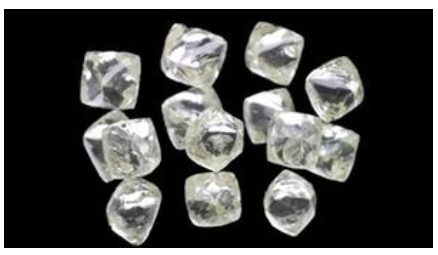
Single and Poly crystal CVD growth Diamond. Low Nitrogen content. Over growth and direction cutting service. 

Device developers can now source diamond materials with specific levels of p-type or n-type dopants, as well as diamond synthesis with C12 and C13 methane for quantum photonics.

Dry film resist for Sandblasting

Negative working Alkaline developable thick Dry film for the sand blast process.

FT 50um and 100um high resolution silicon free. 

Get in Touch

24 hr. service
Call 82-10-6549-9325

Write an email

Call Us

82-32-822-9325

Follow Us:

Address:

ReadyOn Materials

E910-8, 30, Songdomirae-ro,
Yeonsu-gu, Incheon, 21990,
Rep. of KOREA